- 您现在的位置:买卖IC网 > Sheet目录2003 > LTC1427CS8-50#TRPBF (Linear Technology)IC D/A CONV 10BIT W/SMBUS 8-SOIC
6
LTC1427-50
TI I G DIAGRA S
U
W
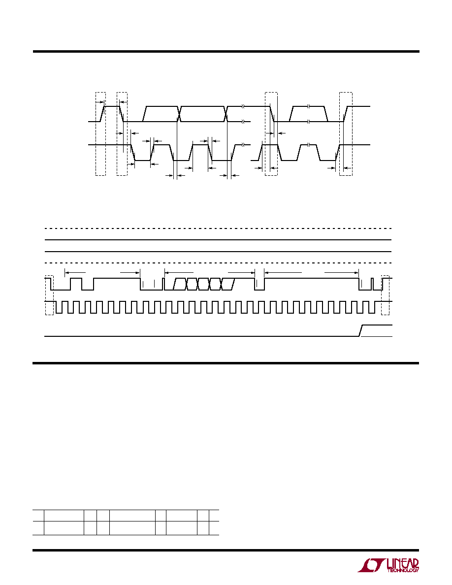
Timing for SMBus Interface
tBUF
tLOW
tHIGH
tr
tf
tHD:STA
tHD:DAT
SDA
SCL
tSU:DAT
tSU:STA
tSU:STO
STOP
1427 TD01
START
STOP
tHD:STA
APPLICATIONS INFORMATION
WU
U
Digital Interface
The LTC1427-50 communicates with an SMBus host
using the standard 2-wire SMBus interface. The Timing
Diagram shows the signals on the SMBus. The SCL and
SDA bus lines must be high when the bus is not in use.
External pull-up resistors or current sources are required
at these lines.
The LTC1427-50 is a receive-only (slave) device. The
master must apply the following Write Byte protocol to
communicate with the LTC1427-50:
1
7
1
181
8
1
S Slave Address WR
A
Command Byte
A
Data Byte
A P
S = Start Condition, WR = Write Bit, A = Acknowledge Bit, P = Stop Condition
IOUT
SCL
S = START
P = STOP
* = OPTIONAL
SDA
AD0
S
1
0
2
1
3
0
4
1
5
1
6
1
7
1
XX
X
1
8
9
10
WR
11
12
13
14
15
16
17
18
19
20
21
22
23
24
25
26
27
P
FULL-SCALE
CURRENT
VCC
GND
VCC
GND
1427 TD02
ZERO-SCALE
CURRENT
*
SHDN
ACK
SMBUS ADDRESS
COMMAND BYTE
DATA BYTE
AD1
Operating Sequence
SMBus Write Byte Protocol, with SMBus Address = 0101111B,
Command Byte = 0XXXXX11B and Data Byte = 11111111B
The master initiates communication with the LTC1427-50
with a START condition (see SMBus Operating Sequence)
and a 7-bit address followed by the write bit = 0. The
LTC1427-50 acknowledges and the master delivers the
command byte. The LTC1427-50 acknowledges and latches
the active bits of the command byte into register A (see
Block Diagram) at the falling edge of the acknowledge
pulse. The master sends the data byte and the LTC1427-
50 acknowledges the data byte. The data byte and last two
output bits from register A are latched into register C at the
falling edge of the final acknowledge pulse and the DAC
current output assumes the new 10-bit data value (see
Block Diagram). A STOP condition is optional. The com-
发布紧急采购,3分钟左右您将得到回复。
相关PDF资料
LTC1428CS8-50#TRPBF
IC D/A CONV 8BIT SINK OUT 8-SOIC
LTC1446LIS8#TRPBF
IC D/A CONV 12BIT R-R DUAL 8SOIC
LTC1448IS8#TRPBF
IC D/A CONV 12BIT R-R DUAL 8SOIC
LTC1450LIG#TR
IC DAC 12BIT R-R PAR MPWR 24SSOP
LTC1451IS8#TRPBF
IC D/A CONV 12BIT R-R 8-SOIC
LTC1454LCN
IC D/A CONV 12BIT R-R DUAL 16DIP
LTC1456CN8
IC D/A CONV 12BIT R-R 8-DIP
LTC1458LIG#TRPBF
IC D/A CONV 12BIT R-R QUAD28SSOP
相关代理商/技术参数
LTC1428CS8-50
功能描述:IC D/A CONV 8BIT SINK OUT 8-SOIC RoHS:否 类别:集成电路 (IC) >> 数据采集 - 数模转换器 系列:- 产品培训模块:Data Converter Fundamentals
DAC Architectures 设计资源:Unipolar, Precision DC Digital-to-Analog Conversion using AD5450/1/2/3 8-14-Bit DACs (CN0052)
Precision, Bipolar, Configuration for AD5450/1/2/3 8-14bit Multiplying DACs (CN0053)
AC Signal Processing Using AD5450/1/2/3 Current Output DACs (CN0054)
Programmable Gain Element Using AD5450/1/2/3 Current Output DAC Family (CN0055)
Single Supply Low Noise LED Current Source Driver Using a Current Output DAC in the Reverse Mode (CN0139) 标准包装:10,000 系列:- 设置时间:- 位数:12 数据接口:DSP,MICROWIRE?,QSPI?,串行,SPI? 转换器数目:1 电压电源:单电源 功率耗散(最大):- 工作温度:-40°C ~ 125°C 安装类型:表面贴装 封装/外壳:SOT-23-8 薄型,TSOT-23-8 供应商设备封装:TSOT-23-8 包装:带卷 (TR) 输出数目和类型:1 电流,单极;1 电流,双极 采样率(每秒):2.7M
LTC1428CS8-50#PBF
功能描述:IC DAC 8BIT SINK OUT 8-SOIC RoHS:是 类别:集成电路 (IC) >> 数据采集 - 数模转换器 系列:- 产品培训模块:Data Converter Fundamentals
DAC Architectures 设计资源:Unipolar, Precision DC Digital-to-Analog Conversion using AD5450/1/2/3 8-14-Bit DACs (CN0052)
Precision, Bipolar, Configuration for AD5450/1/2/3 8-14bit Multiplying DACs (CN0053)
AC Signal Processing Using AD5450/1/2/3 Current Output DACs (CN0054)
Programmable Gain Element Using AD5450/1/2/3 Current Output DAC Family (CN0055)
Single Supply Low Noise LED Current Source Driver Using a Current Output DAC in the Reverse Mode (CN0139) 标准包装:10,000 系列:- 设置时间:- 位数:12 数据接口:DSP,MICROWIRE?,QSPI?,串行,SPI? 转换器数目:1 电压电源:单电源 功率耗散(最大):- 工作温度:-40°C ~ 125°C 安装类型:表面贴装 封装/外壳:SOT-23-8 薄型,TSOT-23-8 供应商设备封装:TSOT-23-8 包装:带卷 (TR) 输出数目和类型:1 电流,单极;1 电流,双极 采样率(每秒):2.7M
LTC1428CS8-50#TR
功能描述:IC DAC 8BIT SINK MICROPWR 8SOIC RoHS:否 类别:集成电路 (IC) >> 数据采集 - 数模转换器 系列:- 产品培训模块:Data Converter Fundamentals
DAC Architectures 设计资源:Unipolar, Precision DC Digital-to-Analog Conversion using AD5450/1/2/3 8-14-Bit DACs (CN0052)
Precision, Bipolar, Configuration for AD5450/1/2/3 8-14bit Multiplying DACs (CN0053)
AC Signal Processing Using AD5450/1/2/3 Current Output DACs (CN0054)
Programmable Gain Element Using AD5450/1/2/3 Current Output DAC Family (CN0055)
Single Supply Low Noise LED Current Source Driver Using a Current Output DAC in the Reverse Mode (CN0139) 标准包装:10,000 系列:- 设置时间:- 位数:12 数据接口:DSP,MICROWIRE?,QSPI?,串行,SPI? 转换器数目:1 电压电源:单电源 功率耗散(最大):- 工作温度:-40°C ~ 125°C 安装类型:表面贴装 封装/外壳:SOT-23-8 薄型,TSOT-23-8 供应商设备封装:TSOT-23-8 包装:带卷 (TR) 输出数目和类型:1 电流,单极;1 电流,双极 采样率(每秒):2.7M
LTC1428CS8-50#TRPBF
功能描述:IC D/A CONV 8BIT SINK OUT 8-SOIC RoHS:是 类别:集成电路 (IC) >> 数据采集 - 数模转换器 系列:- 产品培训模块:Data Converter Fundamentals
DAC Architectures 设计资源:Unipolar, Precision DC Digital-to-Analog Conversion using AD5450/1/2/3 8-14-Bit DACs (CN0052)
Precision, Bipolar, Configuration for AD5450/1/2/3 8-14bit Multiplying DACs (CN0053)
AC Signal Processing Using AD5450/1/2/3 Current Output DACs (CN0054)
Programmable Gain Element Using AD5450/1/2/3 Current Output DAC Family (CN0055)
Single Supply Low Noise LED Current Source Driver Using a Current Output DAC in the Reverse Mode (CN0139) 标准包装:10,000 系列:- 设置时间:- 位数:12 数据接口:DSP,MICROWIRE?,QSPI?,串行,SPI? 转换器数目:1 电压电源:单电源 功率耗散(最大):- 工作温度:-40°C ~ 125°C 安装类型:表面贴装 封装/外壳:SOT-23-8 薄型,TSOT-23-8 供应商设备封装:TSOT-23-8 包装:带卷 (TR) 输出数目和类型:1 电流,单极;1 电流,双极 采样率(每秒):2.7M
LTC1430ACGN
功能描述:IC SW REG CNTRLR STEP-DWN 16SSOP RoHS:否 类别:集成电路 (IC) >> PMIC - 稳压器 - 专用型 系列:- 标准包装:43 系列:- 应用:控制器,Intel VR11 输入电压:5 V ~ 12 V 输出数:1 输出电压:0.5 V ~ 1.6 V 工作温度:-40°C ~ 85°C 安装类型:表面贴装 封装/外壳:48-VFQFN 裸露焊盘 供应商设备封装:48-QFN(7x7) 包装:管件
LTC1430ACGN#PBF
功能描述:IC SW REG CNTRLR STEP-DWN 16SSOP RoHS:是 类别:集成电路 (IC) >> PMIC - 稳压器 - 专用型 系列:- 标准包装:2,000 系列:- 应用:控制器,DSP 输入电压:4.5 V ~ 25 V 输出数:2 输出电压:最低可调至 1.2V 工作温度:-40°C ~ 85°C 安装类型:表面贴装 封装/外壳:30-TFSOP(0.173",4.40mm 宽) 供应商设备封装:30-TSSOP 包装:带卷 (TR)
LTC1430ACGN#TR
功能描述:IC REG SW STEPDOWN 5V HP 16-SSOP RoHS:否 类别:集成电路 (IC) >> PMIC - 稳压器 - 专用型 系列:- 标准包装:43 系列:- 应用:控制器,Intel VR11 输入电压:5 V ~ 12 V 输出数:1 输出电压:0.5 V ~ 1.6 V 工作温度:-40°C ~ 85°C 安装类型:表面贴装 封装/外壳:48-VFQFN 裸露焊盘 供应商设备封装:48-QFN(7x7) 包装:管件
LTC1430ACGN#TRPBF
功能描述:IC SW REG CNTRLR STEP-DWN 16SSOP RoHS:是 类别:集成电路 (IC) >> PMIC - 稳压器 - 专用型 系列:- 标准包装:43 系列:- 应用:控制器,Intel VR11 输入电压:5 V ~ 12 V 输出数:1 输出电压:0.5 V ~ 1.6 V 工作温度:-40°C ~ 85°C 安装类型:表面贴装 封装/外壳:48-VFQFN 裸露焊盘 供应商设备封装:48-QFN(7x7) 包装:管件